

Our Approach
Next-Generation Wireless Receiver Architecture for Base Station Transceivers
Introducing a breakthrough in receiver design for wireless base stations. This section outlines the limitations of existing architectures and presents a new approach using continuous-time bandpass sigma-delta (CTSD) converters.
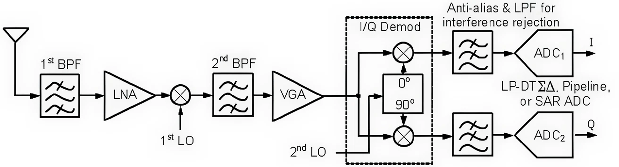
Superheterodyne IQ receivers with pipeline, or SAR (successive approximation) low-pass ADCs mostly applied in consumer smartphones, (LNA = low noise amplifier, VGA = variable gain amplifier, LO = local oscillator, BPF = passive bandpass filter).
Current State of Receiver Architecture
The current receiver architecture in the Wireless Base station is predominantly an adapted heterodyne architecture. The second mixer stage (intermediate frequency to baseband) of this architecture is replaced by a pipelined analog-to-digital converter (ADC) which is operated in sub-sampling meaning the sampling rate of this converter is reasonably smaller than the input frequency of the ADC. The Nyquist criteria are met since the band of interest is located around the IF (intermediate frequency is equal input frequency of pipeline ADC) and is much smaller than the IF. This way one can select one of the higher-order Nyquist bands (e.g. the 10th or 16th) for digitalization by using an ADC with just exactly 1x Nyquist bandwidth.

Heterodyne IF receiver utilizing wide-band Pipeline ADC applied in base stations (2nd mixer already in the digital domain).

Block diagram of LTE (4G) Base station revealing the heterodyne downconverter architecture with a pipeline ADC in sub-sampling mode. Courtesy of RF-Microdevices / QORVO, Janine Love (Aug. 2011)
Sub-Sampling and Analog Filtering Challenges
Sub-sampling introduces new requirements for analog front ends, particularly in anti-aliasing filter design and amplifier noise performance.
The sub-sampling process is moving all signals at the input into the Nyquist band of the output sampling rate. Therefore high order analog filtering is necessary prior to the sub-sampling ADC converter – anti-aliasing filtering. These analog RF filters – mechanical SAW filters – have in-band attenuation and have therefore to be combined with amplifier stages (VGA) to compensate for the in-band attenuation (loss). Additionally to that, the input stage of the sub-sampling converter itself has to have a noise level which takes into account that due to the sub-sampling the noise level of the input stage is increased by the sub-sampling process.

Technological Limitations of Pipeline ADCs
Modern CMOS scaling cannot overcome the analog limitations of pipeline ADC sampling stages.
The sampling input network of the pipeline / SAR ADC is difficult to drive for the preceding amplifier stage since the sampling capacitors of the pipeline input stage have to be charged within the sampling period according to the resolution of the ADC (e.g. 16bit 5GS/s ADC with 5pF => sampling settling to 16bit accuracy within 0,2ns corresponds 11,8τ = 11,8R*C results in 3,4 Ω max. switch resistance over whole voltage swing for all corners).
The sampling process at the input of the pipeline ADC is a technological barrier to the implementation of pipeline ADCs with high signal bandwidth (more than 200MHz) and high resolution (14 ENOB) even in modern nanometer CMOS technologies. The higher bandwidth increases the sampling frequency of the pipelined converter and reduces the settling period for the sampling process. Additionally, the demand for higher ADC resolution increases the settling accuracy which is effective in a further reduction of the settling period. The progress in CMOS process technology speed and the development of process technology with small feature sizes (FinFET) can not overcome this technical limit. The reason is that the analog-to-digital conversion of the continuous-time (CT) analog signal into a discrete-time (DT) signal happens at the input of the pipeline ADC. Therefore the necessary resolution of this process has to be the same as the target resolution of the ADC. Due to the nature of the sampling process, the time constants needed are much higher than the input signal frequencies. Although the CMOS process technology decreased the minimum feature size from 130nm to 3nm in the last 20 years or from 32nm to 3nm in the last 10 years, the resolution and bandwidth of pipeline / SAR ADC did not improve in the same way as needed for example in wireless and radar / Lidar receivers.
CTSD ADC as a New Paradigm
The future lies in digital domain down-conversion enabled by continuous-time sigma-delta architectures.
All the limitations which hinder increasing bandwidth and resolution of the receiver are related to the sampling and down-conversion process of the pipelined converter. This process offers flexibility in down conversion but is very inefficient regarding speed and resolution. To make things worse it can not really benefit from modern process technologies with small feature sizes. Therefore the next evolution of receiver architecture is to digitize the signal first and do the down-mixing process in the digital domain, where it can be done with theoretically unlimited resolution and accuracy. To avoid sampling at the input the signal is digitized with a continuous time bandpass sigma-delta (CTSD) converter which performs the sampling and digitizing after a series of analog gain stages, therefore the sampling error is shaped in the frequency domain and filtered out by the digital post-processing (digital decimation filter: E.Hogenauer 1981, R.Crochiere, L. Rabiner 1975, R.Crochiere, L. Rabiner 1981, B.Brandt, B. Wooley 1994.)

IF receiver utilizing a bandpass CTSD ADC
Bandpass CTSD ADC in Action
The bandpass ADC digitizes only the band of interest in this case the intermediate frequency. All the other signals are filtered out by the analog modulator and the digital post filter. Since the continuous time sigma delta loop anti-alias filtering is part of the ADC all the SAW filter and gain stages in front of the pipeline ADC of current receiver architectures can be omitted. The input stage of the CTSD ADC is equivalent to a time-invariant resistive load (50Ω) and no special driver stage is necessary. The whole IF receiver stage consisting of a series of anti-aliasing filters and gain stages plus pipeline ADC can be replaced by the continuous time bandpass sigma-delta ADC and its digital decimation filter.
The building blocks of this ADC like an analog filter, digital-to-analog converter, internal quantizer, and digital decimation filter benefit to the full extent from new process technologies. Therefore the current and future demand for higher signal bandwidth and higher resolution can be satisfied only with this new wireless receiver architecture.
From Concept to ExecutionContinium’s Role
The concept of Continium Technologies is to design continuous-time bandpass sigma-delta ADCs to enable the customer to build and sell a new wireless base station receiver. The business development and marketing experience as well as customer contacts of the founders show that the 5G customer would since 2020 need a continuous time bandpass ADC with a bandwidth between 400-500MHz, a resolution of 16bit, and an effective number of bits of 13-14 (ENOB).

Proof of Capability
Members of the Continium IC design team already completed the design of the very first 20MHz bandpass CTSD ADC for wireless communication base stations in 2007-2009 and achieved a noise density of -159dBC/Hz and SFDR of 95dBc (programmable IF = 107/173Mhz). The device called ADC16DK161 was stopped during the second prototype tape-out upon acquisition by a giant semiconductor company, circumventing the competition to their obsolete pipeline ADCs.
Vision for Future Applications
The new receiver architecture opens the door to a variety of future ADC products for instance the integration of the mixer stage and the development of an ADC for direct radio frequency digitizing. With decreasing feature size of the process technology, the new wireless receiver architecture will also be used in cell phone receiver or mmWave point-to-point links for wireless backhaul of BTS which offers the possibility to address this market as well as a second step.
Owning the IP and Know-How
Our experience with BTS receiver design traced back to the Xignal startup is that the new receiver architecture is a technology step that is unavoidable and driven by the wireless infrastructure market of recent years. To own the suitable continuous-time bandpass ADC intellectual property (IP) core and know-how together with an experienced team is a very valuable property, independent of the company selling the IP or delivering silicon products.
Barrier to entryWhy Continium Is Ahead
The continuous-time Bandpass Sigma Delta (CTSD) ADC development is extremely complex thus, a typical ADC development team, without any special know-how, would have to spend many years on the learning curve. Because of our experience in research and the product development of CTSD ADCs and our prototype development, we are about 3 years ahead compared to most design teams in the world. Normal ADC design teams who are designing state-of-the-art receiver architectures and Nyquist rate ADCs can be therefore excluded as competitors. The development of this product is in general a very big challenge for a IC development team. It requires best-in-class experts in several very different fields of analog, digital, and mixed-signal IC design. Teams which offer the necessary mixture of experts are at the moment not available and very difficult to establish. In addition, such development involves a very high, and in numbers very difficult to predict, financial risk to companies that have never worked in this field before. These are the reasons why up to now no modern wireless receiver CTSD ADC product for BTS units is available on the market although the customers have been demanding it for at least 10 years.
✷ Strategic significanceOur products align with European objectives
1
To create beyond global state-of-the-art electronics and connectivity solutions enabling the digital transformation by designing Continium’s innovative, power-saving data converters (ADC, DAC) for interfacing the analog domain. Our world is analog (audio, video, sensoric, RF antenna signals), and data converters like ADCs are the key components to digitize these signals for processing in computers. Without high-performance European data converters there will be no digital transformation in Europe. CTSD ADC Architecture
2
For example, in RF wireless signal paths, ADCs are the most valuable elements, since their accuracy affects overall system accuracy. Any ADC errors in the form of non-linearity, distortion spurs or noise can never be eliminated later in digital real-time processing. Data converters are limited by the counteracting fact of speed vs. accuracy, thus innovative CTSD ADC architectures have to be applied to digitize GHz frequency signals for 5G/6G wireless systems. At the same time, we push for the most energy-efficient and resource-sharing electronics by drastically reducing power consumption of data converters through innovative research, opposite to obsolete parallel Nyquist ADCs supplied by giant semiconductor companies, to save energy and help electronics become more eco-friendly.
3
To significantly increase the microelectronics manufacturing footprint for innovative products in Europe by designing innovative data converters in domestic European semiconductor technologies (e.g., X-FAB, GloFo, STmicro) avoiding expensive foreign 3nm-5nm FinFET technologies. By Continium’s “Differentiation by clever Design” using moderate technologies (e.g. 22nm) we will introduce innovation in multichannel MIMO wireless systems and sensorics, potentiated by lowest power consumption and thus allow SMEs to manufacture innovative and competitive products. In this way Continium will strengthen the semiconductor value chain as well as generally Europe-based electronic manufacturability, means increasing the European manufacturing footprint.
Continium’s Design Competencies Offer:
We support you during the semiconductor process technology selection suitable for your product development:
SiGe or CMOS: high-frequency specific foundry vs. general purpose nano-meter scale CMOS or FinFET: evaluating your speed requirements (analog bandwidth, digital interface data rate) we can conclude for optimal nano-meter technology
SOI for RF design and high temperature, high voltage (200V) applications
RF-GaN design of GHz power amplifiers for wireless transmitters
GaN for high voltage (650V) and high current (10A) design with the highest efficiency
We support your product through the supply chain by:
Selecting the proper package (ceramic, flip-chip, chip-on-board) and packaging partner
Ordering wafer lots at your semiconductor foundry
Continium’s test engineers implement the test program for your IC product on the Verigy V93000. ATE test equipment
The Continium’s founders have, in contrast to many other development teams in the world, not only invested a notable amount of effort and time in thorough research work on the topic of analog circuit design, but also spent numerous years on developing ADCs most of which are in high-volume mass production. Their know-how and in-house expertise give Continium Technologies a very strong competitive advantage in notable reductions of development risks. This is recognized as the core value of the company, including the expertise in the fields:
Analog and mixed-signal circuit design:
On average Continium design team has more than 20 years of design experience with different CMOS and BiCMOS technologies all the way down to the lateral SOI 22nm and 3nm FinFET technology nodes.
Fully differential Operational Amplifier based on different topologies: folded cascode Amp, multi-path Amp, telescopic Amp and multipath Amp
Comparators
Reference voltages
Analog continuous-time RC-filter (active RC Filter, Gm-C-Filter)
Current-Mode Circuits (filter, pre-Amplifiers)
Switched Capacitor circuit for data converters, image sensor readout, and filtering (correlated double sampling, Amp finite gain and offset compensation, mismatch cancellation techniques)
Power management: SMPS (switched mode power supplies: DC/DC converter) and LDO regulators
Trouble-shooting your non-functional IC design and improving toward serial production maturity
Digital and Logic Circuit design
SPI/I2C-Interface for data converters (ADC, DAC) and their parameter programming
Digital Post-processing for ADC and DAC (e.g. Parallel-Serial Conversion, Register storage)
Digital Calibration of ADC non-linearity (1.5bit/stage conversion with digital background calibration, time-interleaved ADC inter-channel offset, and gain calibration)
Digital Filter: IIR (Infinite Impulse Response), FIR (Finite Impulse Response), Wave-Digital Filters for Sigma-Delta decimation post-filtering and interpolation pre-filtering
Digital Randomizer/Scrambler for mismatch shaping of DAC converters: DWA (Data Weighted Averaging), DEM (Dynamic Element Matching) algorithms
Switched-Capacitor ADC clock generator (single SC stage non-overlapping clock generation, multi-stage pipeline clock generation, time-interleaved ADC clock generation)
Current steering DAC driving clock for P/N current cells, based on low-crossing and high-crossing latches
Digital algorithm coding in HDL (Verilog, VHDL) and synthesis towards netlist and automated Place&Route layout generation using open source tools for FPGA and ASIC integration
Design Database conversion and post-processing like Netlist converter/translator
Cadence and Mentor/Tanner Design flow interoperability
Simulator netlist conversion scripts:
Tanner Tspice → Synopsys HSPICE
LTspice → Synopsys HSPICE
Netlist converter implemented as AWK script, already implemented and tested, covering the following topics: IF expression, parameter annotations, PWL source annotations, and FUNC functions converted to E/G source elements.
Continium’s test engineers implement the test program for your IC
product on the Verigy V93000. ATE test equipment
◾️ technical resourcesFind out more
An analog approach to compensate for OpAmp offset and finite gain in SC circuitry: A case study of a cyclic RSD ADC
Reprint of the publication from 3rd IEE International Conference on Advanced A/D and D/A Conversion Techniques and their Applications (ADDA’02) Prague, Czech Republic, June 2002
