
12b 1MS/s serial ADC
Effective Number of Bits: 11b (SNDR=68dB signal-to-noise-and-distortion-ratio)
Power supply 3.3V
0.35um CMOS Technology
Low input sampling capacitor of 7pF
Fully differential analog voltage input (3 pins: Vin+, Vin- with adjustable common mode level Vcm)
Layout chip area 0.75mm²
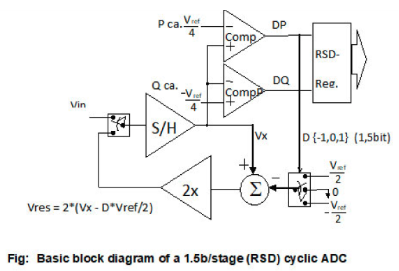
An analog approach to compensate for OpAmp offset and finite gain in SC circuitry: A case study of a cyclic RSD ADC →
Reprint of the publication from 3rd IEE International Conference on Advanced A/D and D/A Conversion Techniques and their Applications (ADDA’02) Prague, Czech Republic, June 2002Abstract: Design of high-resolution Nyquist rate A/D converter necessitates the usage of advanced circuit techniques to compensate for arising analog errors. In switched capacitor ADC, besides the well know techniques such as bottom plate sampling, mismatch-independent and redundant (RSD: 1.5bit/stage) conversion for the elimination of charge injection, capacitor mismatch, comparator and offset sensitivity, respectively, the most utilised circuit techniques are those for OpAmp’s offset and finite gain errors cancellation. An alternative technique for compensation of the errors due to finite gain and offset of Opamp in SC circuits is proposed. This novel method features a charge addition and is compared to so far used approaches based on voltage addition. The concept and the results of a 5V CMOS implementation of cyclic RSD ADC with ratio-independent SC technique using this correction method are discussed.